

Solar energy’s popularity has rapidly increased in the last several years, making a significant impact on the energy market. According to the Solar Energy Industries Association, the U.S. has installed enough solar to power 13.1 million homes and total U.S. solar capacity is projected to more than double by 2024.
As solar energy use becomes more prevalent, so does information about how it’s harnessed and used. Photovoltaic, or solar, panels can often be found in both commercial and residential areas. How are these panels made, and what materials are used to manufacture them?
The table below outlines the raw materials and parts comprising a solar panel.
-
Raw Materials
Silicon is the basic material for conductive electrical components. Before it can be used, it must undergo a treatment process that removes impurities and converts it to pure silicon, or polysilicon. The industry shouldn’t face material shortages any time soon; silicon is abundant, making up one-quarter of the earth’s crust by weight.
-
Ingots & Wafers
Once the silicon is rid of impurities, it is turned into ingots, which are pure silicon cylinders. The ingots are made from a crystal of silicon that is dipped into polycrystalline silicon. The impurities remain in the melted liquid, so the ingot forms as a completely pure cylinder. From there, the ingot is sliced into .5-millimeter-thick wafers, which are shaped into rectangular or hexagonal shapes so they can fit tightly together.
-
Cell
Boron and phosphorus are added to the wafers through a doping process. The wafers are heated in order to allow atoms from these elements, or dopants, to enter the silicon. When these elements are added to the polysilicon, the first result is an excess of electrons, which is then followed by a deficiency of them. This allows the polysilicon to act as a semiconductor.
-
Solar Panels
To conduct a large amount of electricity, many cells must be connected together by electrical contacts. The group is then connected to the receiver. An anti-reflective coating is applied to the panel to prevent loss of sunlight and wasted energy. The cells are then sealed into a rubber or vinyl acetate, framed in aluminum and covered in glass or plastic.
Silicon: Raw Material in Solar Cells
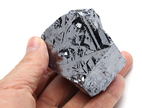
Silicon is the second most common element in the earth’s crust. According to the Minerals Education Coalition, it isn’t found pure in nature; rather, it’s found combined with oxygen in rocks such as obsidian, granite, and sandstone, in a form known as silica. Silicon can be mined from quartzite, mica, and talc, but sand is its most abundant ore source. The silicon in solar panels is manufactured through a reduction process in which the silica is heated with a carbon material and the oxygen is removed, leaving behind purer, metallurgical-grade silicon.
From there, the grade must be further purified into polysilicon, the solar-grade purity of which is 99.999 percent. To yield polysilicons of different grades, several processes may be applied to the element. For electronic-grade polysilicon, which has a higher purity percentage, the metallurgical-grade silicone must pass through hydrogen chloride at extremely high temperatures and undergo distillation. But to yield a solar-grade end product, the silicone goes through a chemical refinement process. In this process, gases are passed through melted silicon to remove impurities such as boron and phosphorus. In its pure form, solar-grade silicon is then turned into cylinders called ingots, which are then sliced into the small conductive pieces that absorb the sunlight in solar panels.
Ingots & Wafers: The Backbone of Solar Cells
Several types of wafers are cut from the ingots: monocrystalline, polycrystalline and silicon ribbons. They differ in terms of their efficiency in conducting sunlight and the amounts of waste they produce.

Monocrystalline wafers are thinly cut from a cylindrical ingot that has a single-crystal structure, meaning that it is comprised of a pure, uniform crystal of silicon. A diamond saw is used to cut the wafers off the cylinder, resulting in a circular shape. However, since circles don’t fit tightly together, the circular wafers are further cut into rectangle or hexagonal shapes, resulting in wasted silicon from the pieces that are removed. According to GreenRhinoEnergy.com, this wasted silicon can be recycled into polysilicon and recut. Researchers are trying to find ways to create monocrystalline cells without so much cutting and waste.
Polycrystalline, sometimes called multicrystalline, ingots are made of multiple crystal structures. They may produce less waste, but they are not as efficient as monocrystalline. The ingots are cube-shaped because they are made from melted silicon poured into a shaped cast. This means the wafers can be cut directly into the desired shape, creating less waste.
Silicon ribbons are thin sheets of multicrystalline silicon. They are so thin that they don’t have to be sliced into wafers. While the thin sheets, or thin films, are flexible, can be used in interesting ways and are less expensive to manufacture, they’re not as durable as wafers and they require more support than other solar panel structures.
Solar Cells: Adding Dopants to Activate the Wafer
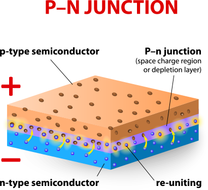
While the silicon wafers are complete at this point, they won’t conduct any energy until they go through the doping process. This process involves the ionization of the wafers and the creation of a positive-negative (p-n) junction. The wafers are heated in cylinders at a very high temperature and put into water. Then the top layer of the cylinder is exposed to phosphorus (a negative electrical orientation) while the bottom layer is exposed to boron (a positive electrical orientation). The positive-negative junction of the cell allows it to function properly in the solar panel.
After this step, only a few more things need to happen in order to create a functioning cell. Because silicon naturally reflects sunlight, there is a considerable risk of losing much of the potential energy from the sun that the cells are supposed to absorb. To minimize this reflection, manufacturers coat the cells with antireflective silicon nitride, which gives the cells the final blue color we see in installed panels.
From there, manufacturers implement a system for collecting and distributing the solar energy. This is done through a silk-screen or screen-printing process in which metals are printed on both sides of the cell. These metals make a roadmap for the energy to travel through on its way to the receiver.
Solar Panels: Assembling Cells Into Useful Devices
Solar panel manufacturers employ different proprietary processes to produce their final solar panel products. But, in general, this is an automated process in which robots do the work. First, the cells must be put together to form a big sheet. According to Solar World, a leading manufacturer of solar panels, its process involves soldering six strings of ten cells each, making a rectangle of 60 cells. Each rectangular matrix is laminated onto glass and quickly becomes a larger panel. From there, the panel needs to be framed so that it is sturdy and protected from any weather it will endure.
In addition, the framing must house the electrical equipment that links the panels together and receives the energy.
Where Does Polysilicon Come From?
Polysilicon has one origin: silica. Silica is mined from the earth and is found in sand, rock, and quartz. Because silica has a dioxide component, it must be taken to a plant, where it is converted to silicon through a heating process. According to the United States Geological Society, there are six domestic companies that produce silicon materials at eight plants. These are all located east of the Mississippi River. Imported silicon comes from all around the world, including China, Russia, Japan, Brazil, South Africa, Canada, Australia, and others.
U.S. Silica Mining and Processing Locations
Source: USGS
How Much Does Raw Silicon Cost?
The most recent data from USGS reports that silicon alloys are a $1.14 billion industry. The silicon metal used in photovoltaic panels cost $1.38 per pound in 2018. According to the USGS Mineral Information Publication, because the production of silicates is so diverse, only a small amount of that industry ties to solar panel creation.
Silicon Production and Mining Facts
-
430,000: Metric tons of silicon mined in 2018 in the U.S.
-
90%: The percent of modules sold today that use silicon.
-
468 billion: Global semiconductor sales in 2018.
-
China, Russia and the U.S. are the biggest silicon producers.
Silicon trends are on the rise and are projected to significantly increase in the next 10 years. This abundant resource comes from numerous countries and has many uses; solar cell production is just one small part. Sources: USGS, U.S. Department of Energy, Semiconductor Industry Association
Resources
Creating Solar Panels
-

Green Rhino Energy This site provides information on the creation of solar cells, with helpful graphics and descriptions.
-

Minerals Education Coalition Find images, history and an easy-to-understand breakdown of information about silica and its uses.
-

U.S. Department of Energy, Lawrence Berkeley National Laboratory Find information about the process of engineering impurities in multicrystalline silicon solar cells.
-

Crystec This site provides manufacturing and equipment information for solar cell and module production.
Solar Energy Information
-

Energy Informative This guide is for homeowners who are considering investing in solar energy, detailing pros and cons of each type of panel.
-

ENF Directory of Polysilicon Manufacturers This is a full directory for everything solar, including panel distributors, manufacturers and installers.
-

PV Education The Photovoltaic Education Network is a hub of resources on photovoltaic panels and energy, designed for educators in these areas.
-

Solar Energy Industries Association This site features research and resources, market breakdowns and discussions of issues and policies affecting the industry.